
Silicon Box cutting-edge, advanced panel-level packaging foundry announces $3.6B investment for expansion into Italy
Silicon Box cutting-edge, advanced panel-level packaging foundry announces $3.6B investment for expansion into Italy
Silicon Box cutting-edge, advanced panel-level packaging foundry announces $3.6B investment for expansion into Italy
Silicon Box cutting-edge, advanced panel-level packaging foundry announces $3.6B investment for expansion into Italy
Silicon Box cutting-edge, advanced panel-level packaging foundry announces $3.6B investment for expansion into Italy
Silicon Box cutting-edge, advanced panel-level packaging foundry announces $3.6B investment for expansion into Italy
Silicon Box cutting-edge, advanced panel-level packaging foundry announces $3.6B investment for expansion into Italy
Silicon Box cutting-edge, advanced panel-level packaging foundry announces $3.6B investment for expansion into Italy
Investment in Northern Italy (Nord Italia), will bring first-of-its-kind, end-to-end chiplet based semiconductor system integration to Europe
- Investment of up to $3.6B (€3.2B) will create approximately 1,600 semiconductor jobs at Silicon Box’s new manufacturing facility, and create thousands of indirect supplier and contract construction jobs
- New Italian facility will enable next generation applications in artificial intelligence (AI), high performance computing (HPC), large language models (LLM), electric vehicles (EV) and automotive, wearables, mobile, smart consumer, edge computing and more by providing advanced packaging and test capacity, anticipated to be in demand in the coming years
- Facilities will be constructed according to green building principles and will operate with high environmental standards to minimize carbon footprint and environmental impact. Silicon Box’s solutions allow greater sustainability through better thermal and electrical performance
- Silicon Box’s investment will align with the Italian government and the European Commission and Union’s goal of a more resilient semiconductor supply chain and to drive innovation
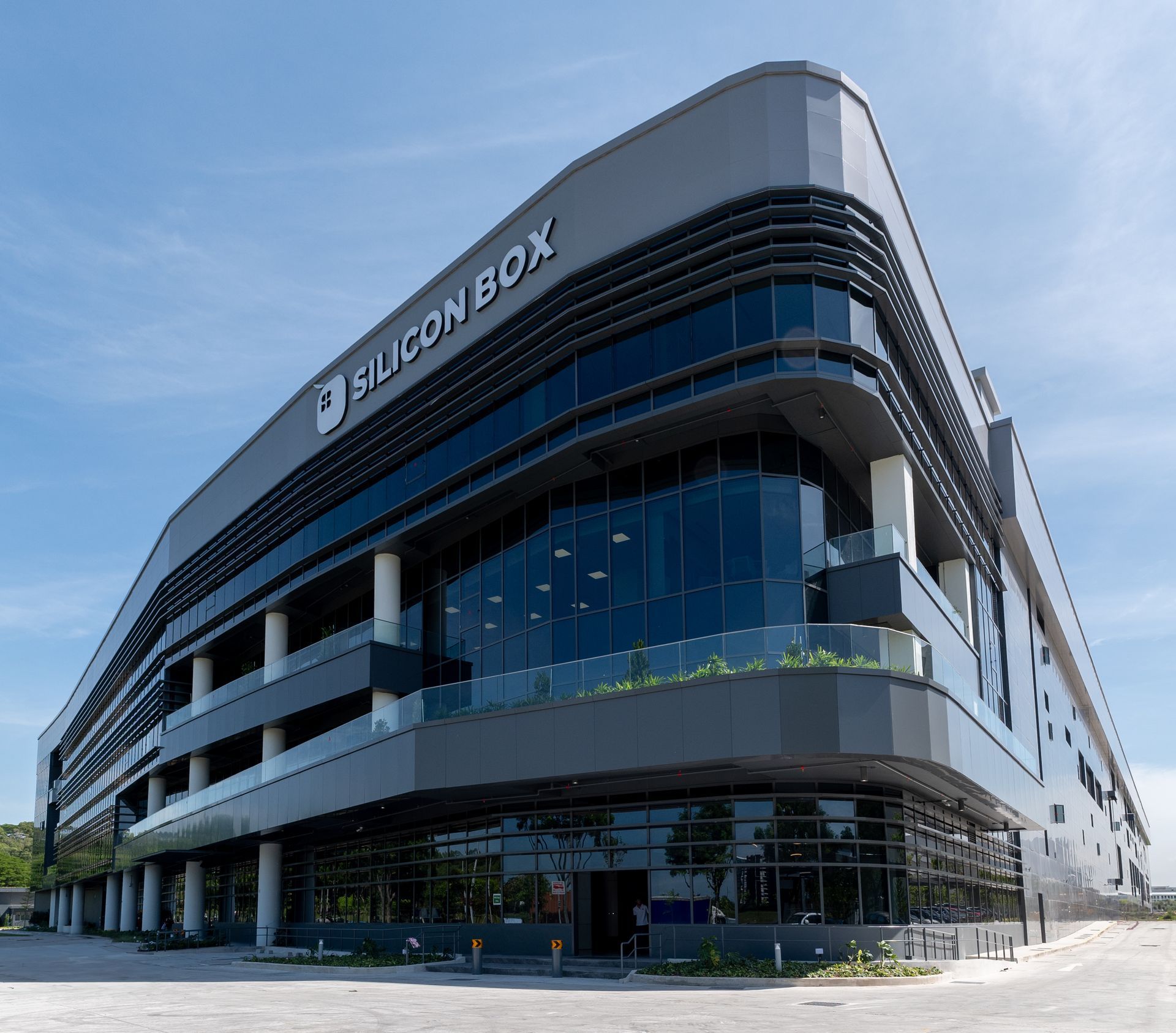
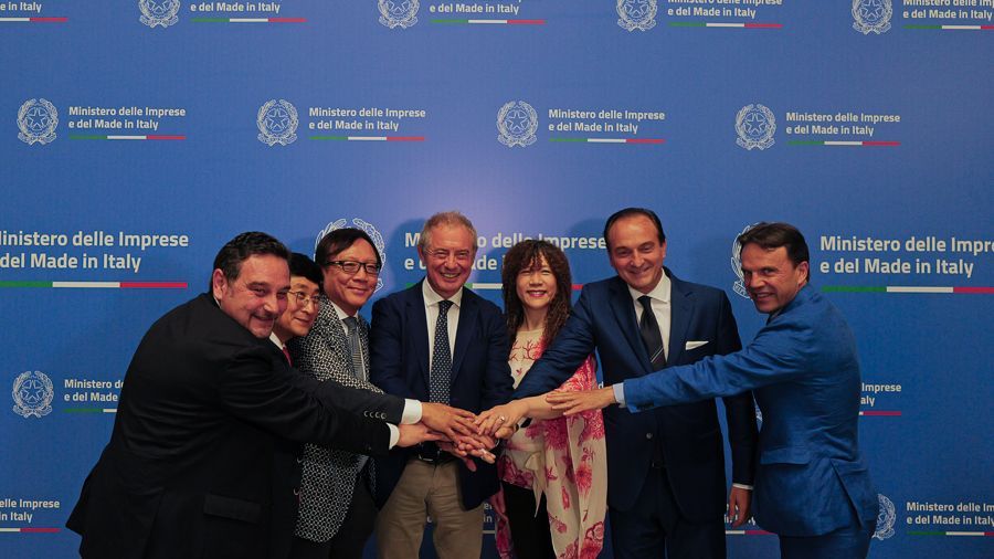
ROME, Italy – 11 March 2024 - Silicon Box cutting-edge, advanced panel-level packaging foundry announced its intention to collaborate with the Italian government to invest up to $3.6B (€3.2B) in Northern Italy, as the site of a new, state-of-the-art semiconductor assembly and test facility. This facility will help meet critical demand for advanced packaging capacity to enable next generation technologies that Silicon Box anticipates by 2028. The multi-year investment will replicate Silicon Box’s flagship foundry in Singapore which has proven capability and capacity for the world’s most advanced semiconductor packaging solutions, then expand further into 3D integration and testing. When completed, the new facility will support approximately 1,600 Silicon Box employees in Italy. The construction of the facility is also expected to create several thousand more jobs, including eventual hiring by suppliers. Design and planning for the facility will begin immediately, with construction to commence pending European Commission approval of planned financial support by the Italian State.
As well as bringing the most advanced chiplet integration, packaging, and testing to Italy, Silicon Box’s manufacturing process is based on panel-level-production; a world leading, first-of-its-kind combination that is already shipping product to customers from its Singapore foundry. Through the investment, Silicon Box has plans for greater innovation and expansion in Europe, and globally. The new integrated production facility is expected to serve as a catalyst for broader ecosystem investments and innovation in Italy, as well as the rest of the European Union.
“We believe innovation is driven by cultural values that embrace curiosity, passion, and a tireless commitment to excellence,” said Dr. Byung Joon (BJ) Han, co-founder and CEO of Silicon Box. “Italy was one of our top choices for global expansion because we found that its culture shares our values. We have seen great promise through our collaborations with the Italian government and various regional, institutional and commercial stakeholders to date, which we know will be necessary to successfully execute this first-of-a-kind project in Europe.”
“We are excited to bring Italy to the forefront of chiplet deployment and the semiconductor industry, through this investment into the world’s most advanced packaging solution. It will enhance competitive strengths in design, artificial intelligence (AI), large language models (LLMs), electronic vehicles (EVs) and automotive, mobile, wearables, smart consumer, edge computing, and material sciences of the Italian ecosystem, and revolutionize Europe’s position in the global [semiconductors] supply chain,” said Dr. Sehat Sutardja, co-founder and Chairman of Silicon Box. “Throughout my career, I have always been a big believer in Italian and European ingenuity.”
Advanced Packaging to Drive Innovation across Italian and European Semiconductor Ecosystems
“Italy was chosen as the location for Silicon Box’s first global expansion for several reasons, including its infrastructure, strong talent base and the government’s initiative to support and streamline the business environment and key stakeholder conversations,” said Dr. Han. “The competitive jobs that Silicon Box’s new facility will create will include engineers, equipment technicians, factory operators, and business functions. Italy offers an exceptional ecosystem for higher education with strong traditions in various engineering disciplines. This was a decisive factor in Silicon Box’s choice to build in Northern Italy and will be essential to our long-term success.”
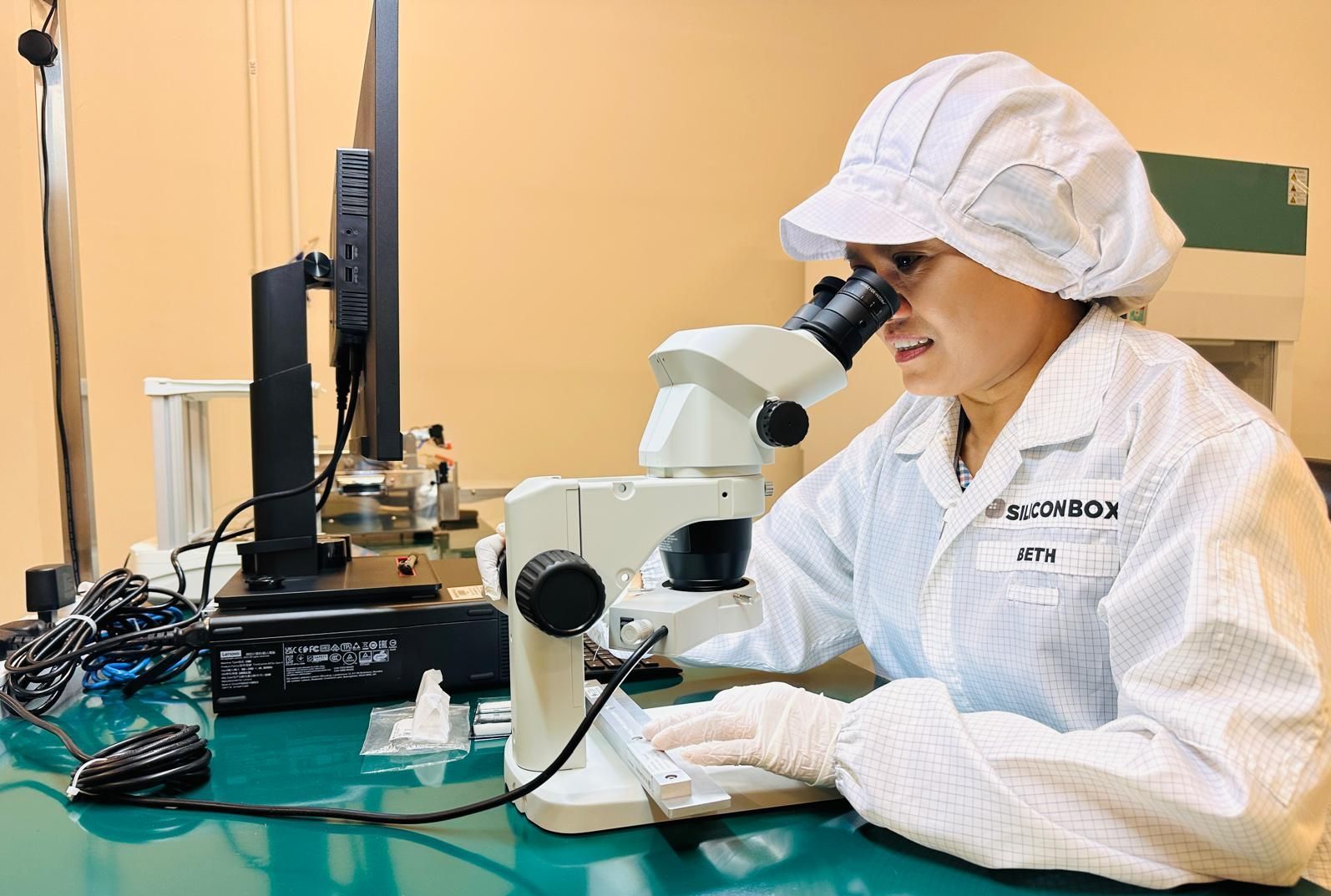
Wafer fabrication facilities, often referred to as “fabs”, create chips on silicon wafers through various advanced processes. Packaging facilities, such as the one planned for Italy by Silicon Box, receive completed wafers from fabs, cut them into individual chips, assemble or “package” them into final products and test them for performance and quality. The finished or packaged chips are then shipped to customers which include specialty chip design companies, integrated device manufacturers (IDMs) and original equipment manufacturers (OEMs).
Notably, Silicon Box facilities specialize in advanced chiplet integration capabilities (“advanced packaging”), on a large manufacturing format for scale. The chiplet concept is an alternative to traditional semiconductor manufacturing, which focused on building entire systems-on-chips (SoCs) on silicon wafers, then moving to conventional packaging processes. Chiplets describe manufacture of individual system modalities as standalone chips or chiplets on a wafer, then integrating these separate functionalities into a system through advanced packaging, creating a system-in-package (SiPs). With this, advanced packaging technology comes to the forefront of semiconductor manufacturing innovation, in a new paradigm for the industry.
The chiplet concept itself was introduced by Silicon Box co-founder Dr. Sutardja at the International Solid State Circuits Conference (ISSCC) in 2015, where he was plenary speaker. Dr. Han is the inventor of semiconductor packaging solutions fundamental to enable chiplets through advanced packaging. Their collaboration has been the basis for Silicon Box’s record-breaking progress as a company in the semiconductor manufacturing space, traditionally dominated by a few large companies.
Bringing Resilience and Sustainability to the SemiconductorSupply Chain, and Enabling Advanced AI Technology and Ecosystems in Europe
“Silicon Box’s new foundry in Italy will be able to accept wafers from all foundries and support a wide variety of customers, worldwide, through its innovative approach,” said Mike Han, Silicon Box’s Head of Business. “The location is well suited to work with Europe’s existing and planned semiconductor wafer fabrication clusters in Italy, Germany, and France. Proximity will enable close collaboration from design through to final manufacturing, and help increase resilience and cost efficiency of the European and global semiconductor supply chain, at a time when there is a global shortage for this type of technology.”
“Silicon Box’s investment in Italy can act as a catalyst for further investments by ecosystem companies and for building and attracting the talent needed to support a thriving European semiconductor industry,” co-founder Weili Dai said. “It will also enable existing Italian and European semiconductor interests to maximize their existing core competencies and drive further efficiency and innovation through the creative and cost-efficient deployment of advanced packaging and chiplet architecture to support their own strategic objectives. This is particularly significant for the development of native artificial intelligence, large language models, supercomputers, mobile, wearables, smart factories, and edge computing companies.”
“This new Silicon Box AI-powered smart factory will be the first to showcase the ecosystem’s technology end-to-end; from initial design and construction to full process automation, as well as employee and customer training from our comprehensive digital twin. This will facilitate seamless expansion, employee and customer immersion, and groundbreaking efficiencies in management and performance monitoring,” she added.
Recent global disruptions emphasize the need to build a more resilient supply chain for semiconductors in Europe. Silicon Box supports the European Commission’s goal to reclaim 20 percent of global semiconductor manufacturing capacity by 2030, and is committed to supporting a vision of a global semiconductor supply chain that is resilient and geographically balanced.
Silicon Box built it’s first advanced packaging facility in Singapore within a year, and began shipping finished products to customers three months after the factory’s grand opening, showcasing unique capability for fast project execution, which will also apply to the Italian factory.
Silicon Box’s products and practices are committed to sustainability and will adhere to high environmental standards across its global operations. This will also apply to Silicon Box’s first global facility in Northern Italy. This facility will be constructed and managed according to Europe’s net zero principles, minimizing its carbon footprint and the impact on the environment.
Forward-Looking Statements
This press release contains forward-looking statements that involve a number of risks and uncertainties. Such statements include: our manufacturing expansion and investment plans and expectations in the European Union (EU) and the anticipated benefits therefrom; anticipated supplier, ecosystem, community, and government support and approval for our planned EU investments and anticipated benefits related to such support; environmental plans for and benefits from our factories and technologies; and other characterizations of future plans, expectations, events, or circumstances.
Such statements involve risks and uncertainties that could cause our actual results to differ materially from those expressed or implied, including: changes in demand for our products; Silicon Box’s failure to realize the anticipated benefits of its strategy, plans, and proposed transactions; construction delays or changes in plans due to business, economic, or other factors; increases in capital requirements and changes in capital investment plans; adverse changes in anticipated government incentives and associated approval related to Silicon Box’s planned EU investments; adverse legislative or other government actions; insufficient ecosystem support; the impact of macroeconomic and geopolitical trends and events; and other risks and uncertainties described in this press release.
All information in this press release reflects management’s views as of the date hereof, unless an earlier date is specified. We do not undertake, and expressly disclaims any duty, to update such statements, whether as a result of new information, new developments, or otherwise, except to the extent that disclosure may be required by law.
About Silicon Box
Silicon Box is an advanced semiconductor packaging company, specializing in cutting-edge integration technology and manufacturing processes. We offer solutions that enable chiplet architecture, as well as high performance alternatives to traditional packaging schemes. Leveraging our proprietary technology, 30 years of multi-sectoral expertise, and relationships with best-in-class partners, we strive to solve the unique challenges of chiplet adoption in order to build the emergent technologies shaping the world around us today.
Silicon Box was founded in 2021 by Dr. Byung Joon (BJ) Han, Dr. Sehat Sutardja and Weili Dai. Dr. Han was previously the Chairman, CEO and CTO of the world’s 3rd largest outsourced assembly and test provider, STATS Chippac (SSE: 600584) for two decades, taking the company to $4B in revenue during his tenure. Dr. Han is the inventor of many of the most advanced packaging solutions in today’s market, and his team at Silicon Box holds standing records for yield in advanced packaging technology at wafer level production. Dr. Sutardja introduced the concept of chiplets at the International Solid-State Circuits Conference (ISSCC) in 2015. He and Weili Dai founded Marvell Technology Group (NASDAQ: MRVL) in 1995, and ran the company for twenty years from a start-up to an over $50B market value company.
For press enquiries, email
media_enquiries@silicon-box.com

Chipping In: Billionaire-Founded Unicorn Startup Makes Semiconductor ‘Chiplets’ For The AI Boom
Singapore-based Silicon Box specializes in chiplets...
Singapore Startup to Invest €3.2 Billion in Italy Chips Factory
Semiconductors startup Silicon Box will invest €3.2 billion ($3.5 billion) in Italy...
Silicon Box investirà 3,2 miliardi per un nuovo sito in Italia
Silicon Box invests EU3.2 million towards a new factory in Italy

Silicon Box to invest $3.5 billion in new chip plant in Italy
... in a new plant in northern Italy under a government-backed deal, the Italian industry ministry said...

Marvell founders launch $2 bln chips foundry in Singapore
The two-year old startup said in a statement that the 73,000-square metre factory would create over...

Silicon Box investe in Italia, 3 mld per fabbrica microchip
Silicon Box investe in Italia, 3 mld per fabbrica microchip
Silicon Box investirà 3,2 miliardi in Italia per la produzione di chiplet
punta sul nostro Paese con un impianto di soluzioni per la produzione di “porzioni” di microchip

Silicon Box announces $3.6B investment for expansion into Italy
Investment in Northern Italy (Nord Italia), will bring first-of-its-kind, end-to-end chiplet based semiconductor system integration to Europe

Silicon Box cutting-edge, advanced panel-level packaging foundry announces $3.6B investment for expansion into Italy
Investment in Northern Italy, will bring first-of-its-kind, end-to-end chiplet based semiconductor system integration to...
Reg. No.: 202117750K
ISO 9001:2015
Contact Us
20 Tampines Industrial Avenue 3, Singapore 529580
customer_enquiry@silicon-box.com
supplier_enquiry@silicon-box.com
All Rights Reserved | Silicon Box Pte Ltd
We use cookies to ensure that we give you the best experience on our website. To learn more, go to the Privacy Page.