
Silicon Box launches $2 billion, state-of-the-art advanced semiconductor packaging fab in Singapore to accelerate the future of computing and the AI Era
Silicon Box launches $2 billion, state-of-the-art advanced semiconductor packaging fab in Singapore to accelerate the future of computing and the AI Era
Silicon Box launches $2 billion, state-of-the-art advanced semiconductor packaging fab in Singapore to accelerate the future of computing and the AI Era
Silicon Box launches $2 billion, state-of-the-art advanced semiconductor packaging fab in Singapore to accelerate the future of computing and the AI Era
Silicon Box launches $2 billion, state-of-the-art advanced semiconductor packaging fab in Singapore to accelerate the future of computing and the AI Era
Silicon Box launches $2 billion, state-of-the-art advanced semiconductor packaging fab in Singapore to accelerate the future of computing and the AI Era
Silicon Box launches $2 billion, state-of-the-art advanced semiconductor packaging fab in Singapore to accelerate the future of computing and the AI Era
Silicon Box launches $2 billion, state-of-the-art advanced semiconductor packaging fab in Singapore to accelerate the future of computing and the AI Era
With chiplets at the forefront of semiconductor integration, the factory is ready to support its global customers and partners.
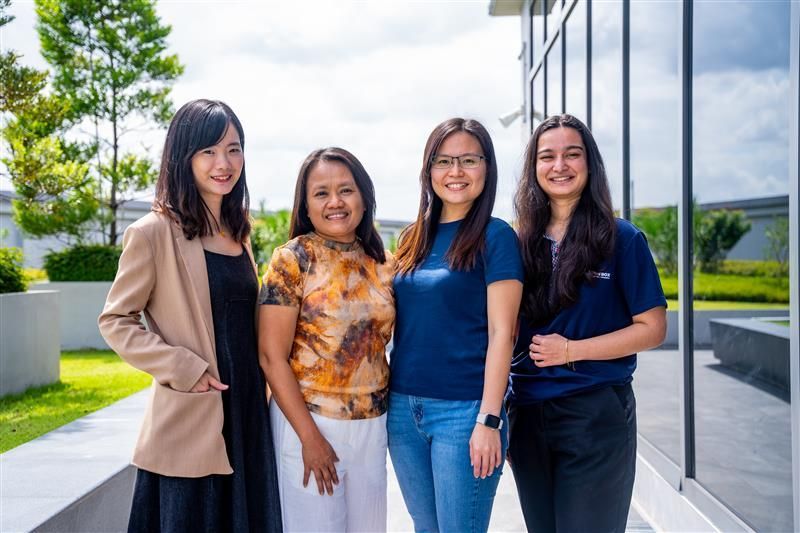
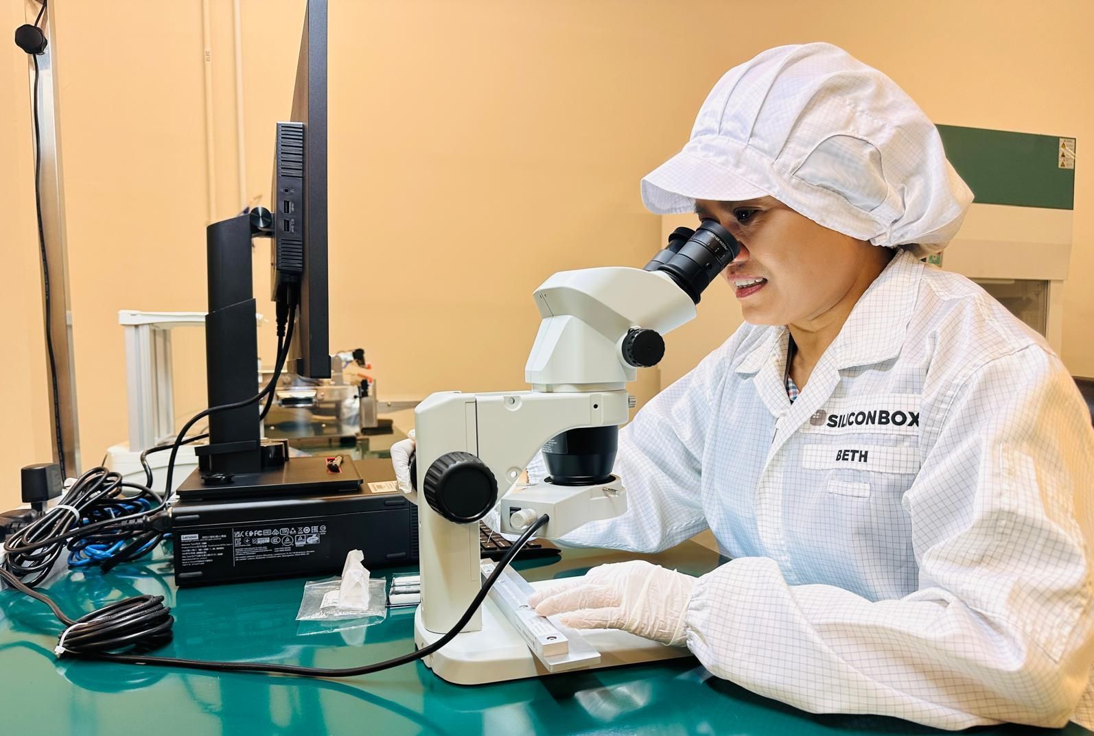
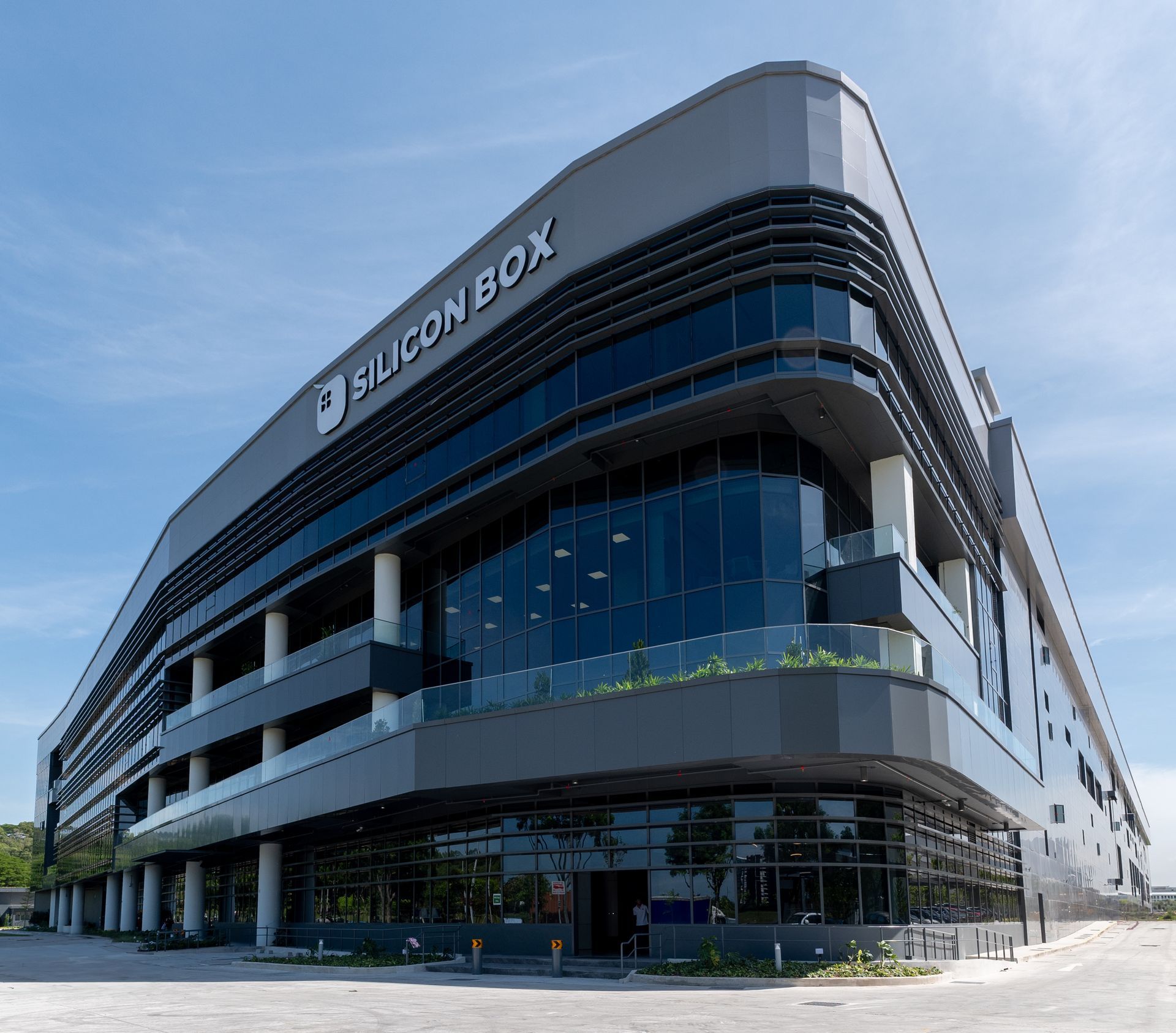
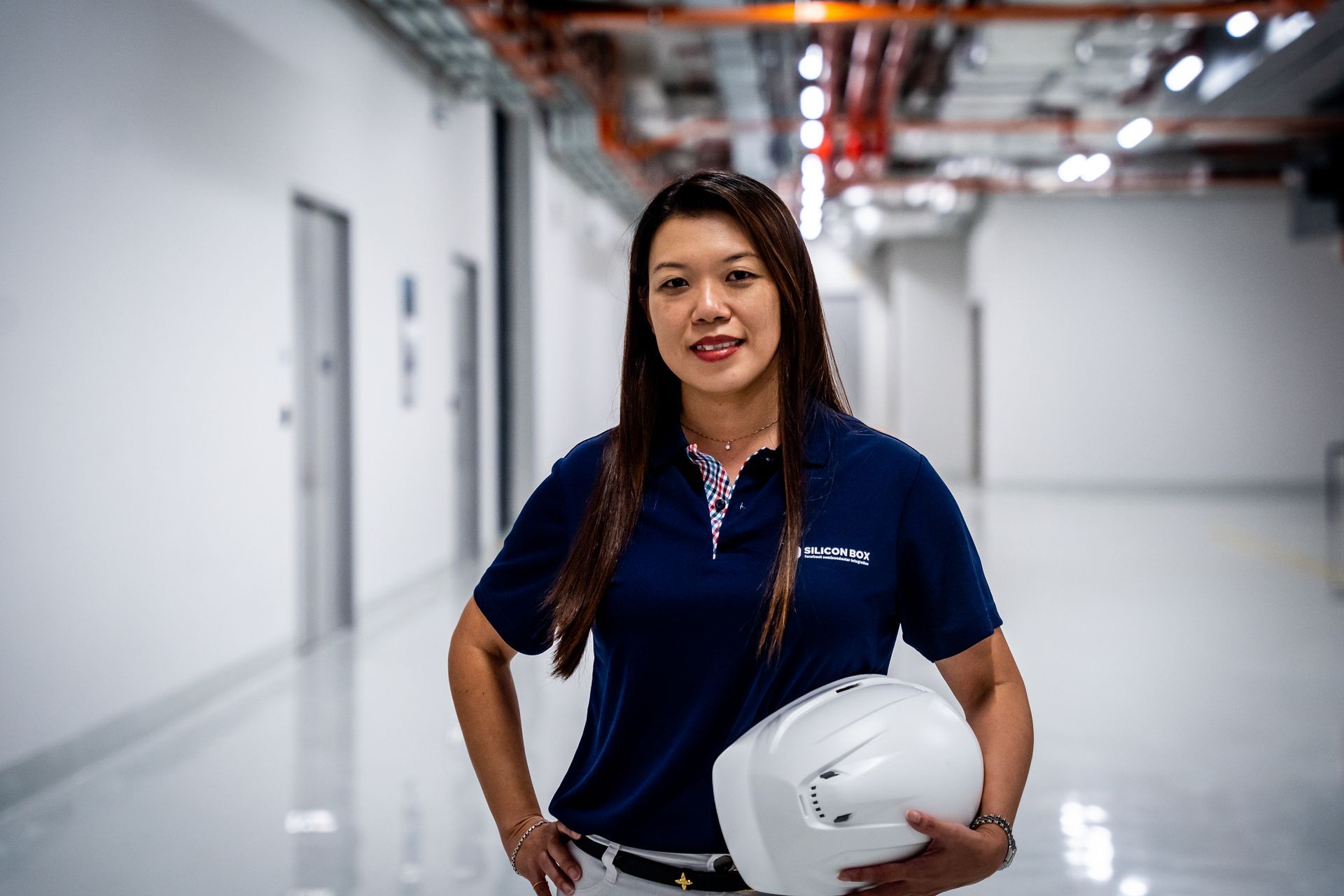
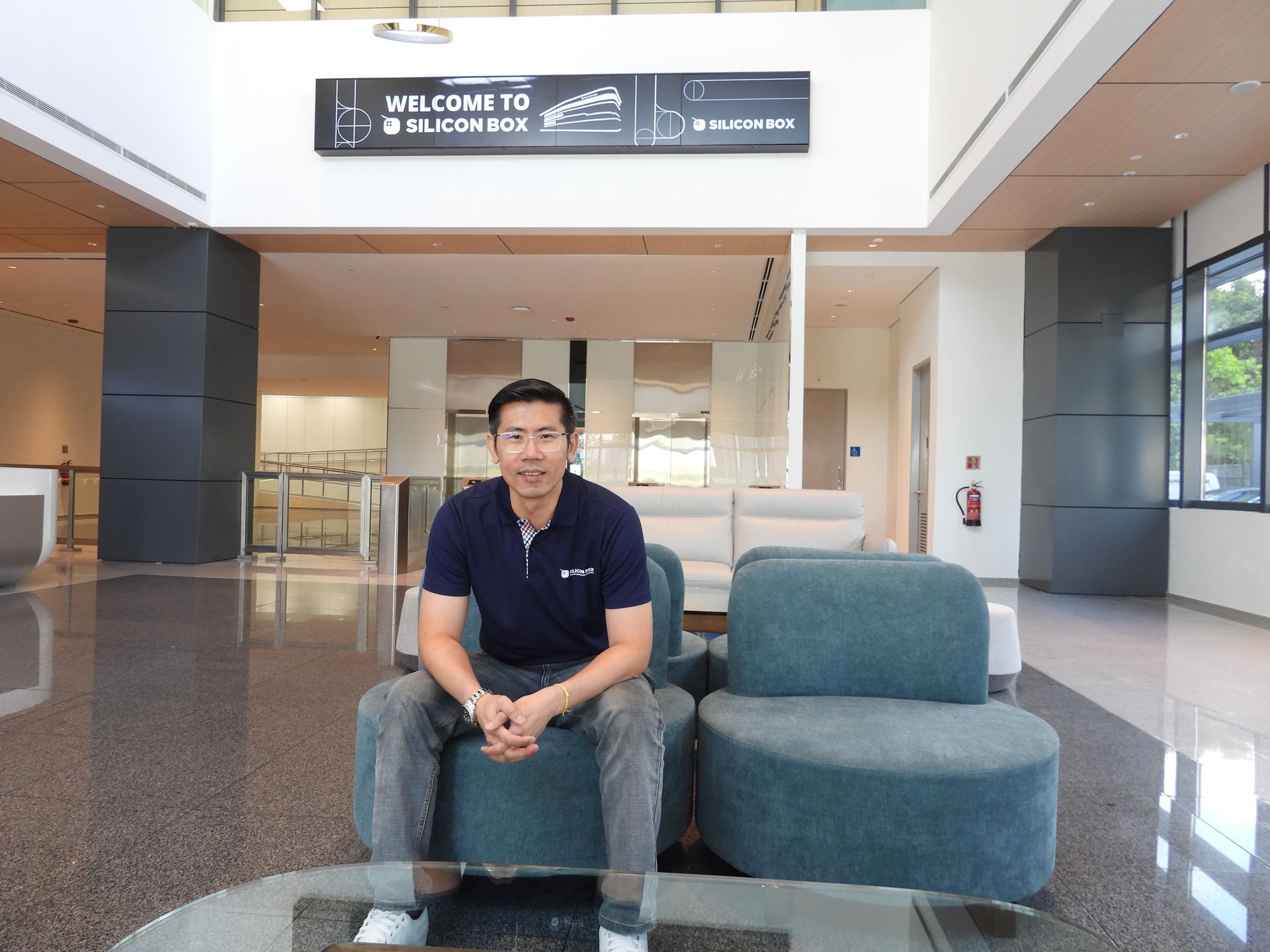
Singapore, July 2023 – Silicon Box, a cutting-edge semiconductor startup, today unveiled its SGD 2 billion advanced semiconductor packaging fab aimed at revolutionising the chip manufacturing sector, developing local capabilities, and boosting Singapore’s position as a global hub for semiconductor manufacturing. Silicon Box will hire and train thousands of high-level employees, with the support of the Singapore Economic Development Board (EDB).
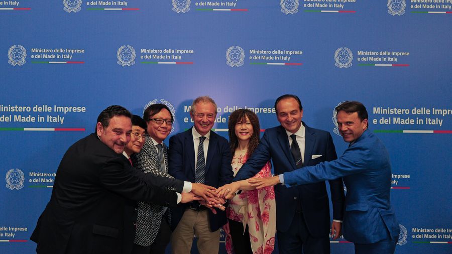
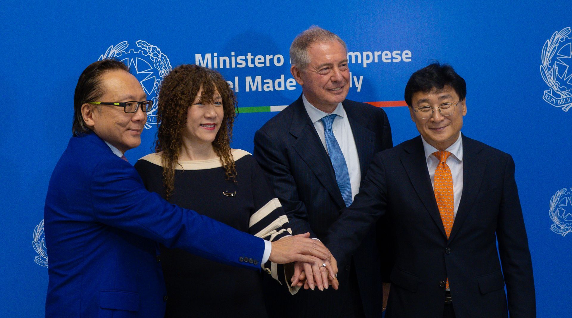
The grand opening ceremony of the 73,000 sqm facility in Tampines, the size of 15 football fields, was graced by Mr Png Cheong Boon, Chairman EDB, and the company’s three co-founders Dr. Han Byung Joon - Chief Executive Officer of Silicon Box - Dr. Sehat Sutardja - Chairman of the board, and Weili Dai.
“Silicon Box is well poised to solve the unique challenge for chiplets, which are essential to power emergent technologies. Our team of experts with over 30 years of experience, critical ecosystem of partners, and proprietary interconnection technology will shorten the design cycle of chiplets, lower new device costs, reduce power consumption and enable faster-time-to-market for industry partners involved in areas such as artificial intelligence (AI), data centres, electronic vehicles (EVs), mobile, and wearables” Dr. BJ Han says.
“At MeetKai, we are thrilled to have partnered with Silicon Box and have barely touched the surface of what promises to be very fertile ground for enterprise and industrial use cases in the metaverse. As a disruptive leader in the metaverse space, it gives us great pride to work with a company moving so disruptively in the Semiconductor space. Our heavy usage of AI has given us a first hand look at the needs for mass disruption in the semiconductor space. By automating training and monitoring capabilities, we hope to set the groundwork for Silicon Box to scale to many more factories even faster,” said MeetKai Co-Founder and CEO, James Kaplan. “Using advanced AI-powered and metaverse technologies, we were able to create a full digital twin of Silicon Box’s state of the art advanced packaging fab in a matter of days, providing the capabilities for professional training, orientation tours, and live creative collaboration at fractions of the cost and time that were previously thought possible.” Created by meetkai
Transforming the semiconductor industry with advanced chiplet interconnection technology
Despite its wide potential and high demand across emerging technologies, deployment of chiplets continues to face challenges with manufacturing capacity, complexity and cost.
“The concept of chiplets – building larger systems on chips with modular components produced at scale – allows us to enable chip designers to focus on optimizing for performance and low power consumption in large chip designs, at a cost that is not prohibitive,” Dr. Sehat Sutardja explains. “Silicon Box’s proprietary fabrication method, sets a new standard for design flexibility and electrical performance at low cost. This agility in semiconductor design cycles enables the industry to take advantage of the chiplet concept and bring designs that double computing performance, at up to four times lower costs for graphical processors and high-performance computing chips, and up to half the cost for more widely consumed mobile processors.”
World Class Partnerships and Global Industry Adoption
Silicon Box has formed partnerships globally with industry leaders to enable semiconductor solutions required to power next generation applications. “What the users of tomorrow will expect when it comes to their end experience, whether it is on a mobile device, electric vehicle, or an end application utilizing generative AI, requires fundamentally different approaches to semiconductor manufacturing such as the advanced panel level packaging technology in which Silicon Box stands at the forefront. ” Co-Founder Weili Dai added. “We founded Silicon Box to meet this demand. This is our first multi billion dollar factory and we are eager to scale rapidly to support our customers and partners, globally. Many of these customers and partners have come to the Grand Opening to celebrate this key moment for Silicon Box and the industry, with us. We believe this is a testament to the faith they have in our capability.”
Jodi Shelton, CEO of the Global Semiconductor Alliance, showed the industry's far reaching support with her attendance adding, “I’m very proud to be part of this launch and celebration, at the Grand Opening. Seeing the factory, what the team has accomplished, and their decades of industry leadership, track record, and success, leaves me very optimistic about the future of Silicon Box, and what it means for the global industry.”
Developing talent for qualitative transformation of the manufacturing sector
Digitalisation, accelerated by the pandemic, has increased demand for talent in high-end engineering. Leveraging the combined expertise and patents of the co-founders of Silicon Box and commitment to R&D, the startup aims to attract the brightest minds and digital experts to join the innovative team at the facility. In collaboration with EDB, Silicon Box will be providing training opportunities for graduates from institutes of higher learning to contribute to the development of radical new technologies to meet this demand.
Silicon Box is a Singapore-based, global champion in semiconductors that will bring the city-state to the forefront of innovation in the space. It will help facilitate further development of native supply chains and technologies for this critical industry.
EDB’s Chairman Png Cheong Boon said, “Singapore is home to a vibrant and sophisticated semiconductor industry, with a strong ecosystem of solution providers and partners. Silicon Box’s decision to set up its first manufacturing and R&D facility in Singapore is testament to our competitiveness as a critical global node for semiconductors, and a vote of confidence in the long-term growth prospects of the sector in Singapore. We will continue to strengthen our industry’s competitiveness by developing a stronger talent pipeline, reducing the sector’s carbon footprint and deepening our semiconductor R&D capabilities.
JTC’s Director of Biomedical & Electronics Cluster Group Mr Cheong Wee Lee said, “Silicon Box brings its cutting-edge design capabilities and proprietary packaging system in chiplets to an established semiconductor ecosystem at Tampines Wafer Fab Park, where it can collaborate and build partnerships with industry players. We are pleased to support Silicon Box in the development of its purpose-built facility which will house R&D and manufacturing functions under one roof, enabling it to ramp up operations quickly and shorten time-to-market to meet customer demands.”
End-to-end commitment on economic resource efficiency at scale
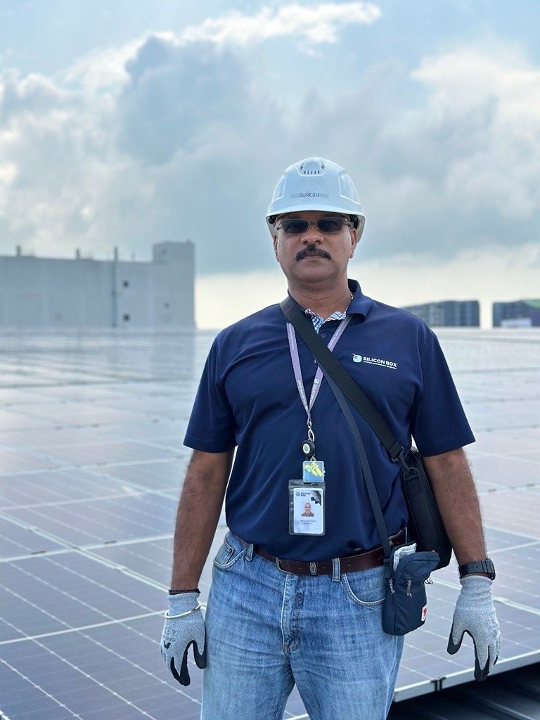
Operating with economically sound processes to minimise the negative effects on the environment, Silicon Box ensures that its interconnected chiplets are energy efficient at scale. Built with resource efficiency in mind in keeping with industry best practices, the facility includes:
- A Reverse Osmosis De-Ionized (RO-DI) water filtration system that purifies NeWater for manufacturing processes.
- Fully contained wastewater treatment facility enables 50% of post-manufacturing waste water to be recycled and reused.
- Multi-grid voltage system and solar panels improve the capacity of transmission lines and distributes power consumption more efficiently.
- Energy efficient window glass and blinds, coupled with high-quality insulation, reduces energy required for cooling.
About Silicon Box
Silicon Box is an advanced chiplet interconnection company specialising in cutting-edge advanced semiconductor packaging. Founded in 2021 by Dr. BJ Han, Dr. Sehat Sutardja, and Ms. Weili Dai, the Singapore company is capable of collaborating on everything from initial design to final manufacturing of chiplets through its established relationships with best-in-class partners, has a track record of customer success and proprietary technology. Its state-of-art facility in Singapore provides advanced interconnection capabilities and demonstrates leadership in innovation at this critical epoch of semiconductor manufacturing technology. To learn more about Silicon Box, visit www.silicon-box.com
About MeetKai Inc.
MeetKai Inc. is a Metaverse and Artificial Intelligence company based in Los Angeles, California. Listed by Forbes as a leading innovator in the space, MeetKai's cutting-edge AI can give personalized results in a natural conversation and boast expertise about any subject inside the metaverse. After reaching 50+ million users worldwide, MeetKai launched the most cost-effective and easy-to-use metaverse creation tools in the market and is currently building virtual worlds rooted in reality and true utility, accessible to everyone, via browser. Visit
www.meetkai.com for more info and the latest MeetKai news.
Press and Interview Enquiries
jan@bulletboadcast.io or vicki@bulletbroadcast.io
Investor Enquiries
Michael Han, Head of Business | mike.han@silicon-box.com
Reg. No.: 202117750K
ISO 9001:2015
Contact Us
20 Tampines Industrial Avenue 3, Singapore 529580
customer_enquiry@silicon-box.com
supplier_enquiry@silicon-box.com
All Rights Reserved | Silicon Box Pte Ltd
We use cookies to ensure that we give you the best experience on our website. To learn more, go to the Privacy Page.