Advanced packaging facility in Piedmont to bring first-of-a-kind semiconductor manufacturing capabilities to Europe, enable chiplet architecture
- Silicon Box selects site near Novara, in Piedmont, as location for advanced packaging facility, planned to begin construction mid- 2025 and to begin production in 2028
- Investment of up to €3.2B ($3.6B) will create approximately 1,600 semiconductor jobs at Silicon Box’s new manufacturing facility, and create thousands of indirect supplier and contract construction jobs
- New Italian facility will enable next generation applications in artificial intelligence (AI) supporting large language models (LLM), high performance computing (HPC), electric vehicles (EV) and automotive, wearables, mobile, smart consumer, edge computing and more by providing advanced packaging and test capacity, anticipated to be in demand in the coming years
- Silicon Box’s investment will align with the Italian government and the European Commission and Union’s goal of a more resilient semiconductor supply chain and to drive innovation
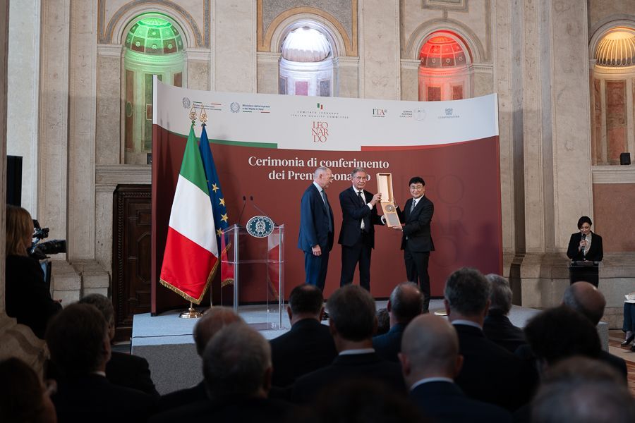
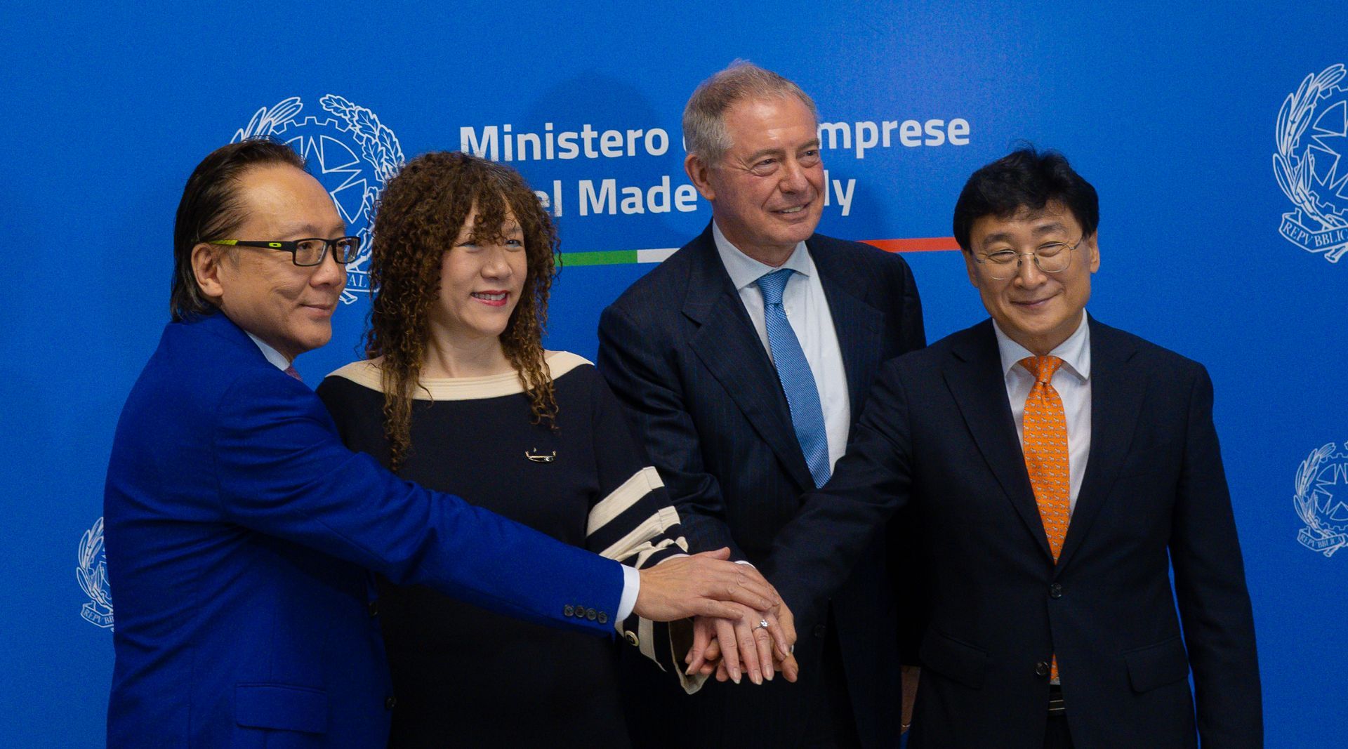
ROME, Italy – The co-founders of Silicon Box, CEO Dr. Byung Joon (BJ) Han, Dr. Sehat Sutardja, and Weili Dai, together with the Minister Adolfo Urso, Presidente Alberto Cirio of the Piedmont region, and Mayor Alessandro Canelli of the municipality of Novara today announced that Novara in Piedmont will be the site of the company’s new, first-of-a-kind advanced semiconductor packaging and testing foundry. The parties signed a letter of intent outlining their commitment for collaboration related to the site and investment, this morning, at the Ministry of Enterprises and Made in Italy in Rome, subject to the European Commission approval of the planned financial support to be granted by Italy.
The site in Novara and Piedmont was selected from a shortlist of sites and regions in Northern Italy (Nord Italia) through a detailed evaluation process. This effort aimed at ensuring that selection be aligned with the requirements and conditions necessary for the planned facility, and prior commitments agreed between Silicon Box and the Italian government.
“Silicon Box’s advanced packaging facility in Novara is expected to create up to 1,600 highly paid jobs and bring first-of-a-kind advanced semiconductor packaging and testing capabilities to Italy, and to Europe,” said Dr. Byung Joon Han, CEO and cofounder of Silicon Box. “We appreciate the cooperation of all the sites, municipalities and regions that participated in our evaluation process. Every site was carefully reviewed and considered, and each had its own independent merits that reinforced our decision to build in Italy.”
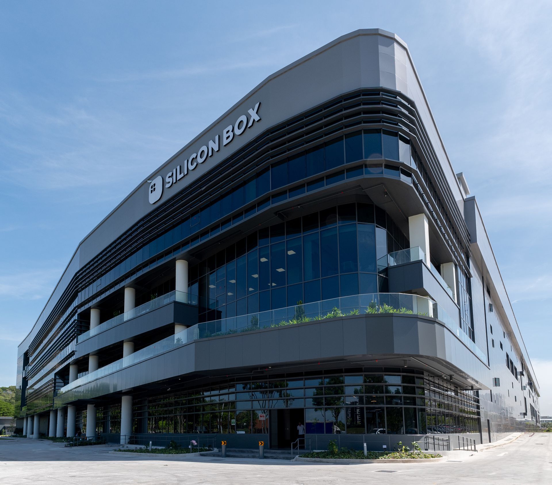
Earlier this year, Silicon Box announced its intention to collaborate with the Italian government to invest up to €3.2B ($3.6B) in Northern Italy, as the site of a state-of-the-art semiconductor assembly and test facility. The facility will help meet critical demand for advanced packaging capacity to enable next generation technologies that Silicon Box anticipates by 2028. The multi-year investment replicates Silicon Box’s flagship foundry in Singapore, which has demonstrated capability and capacity for the world’s most advanced semiconductor packaging solutions, before further expansion into 3D integration and testing. The new integrated production facility is expected to serve as a catalyst for broader ecosystem investments and innovation in Italy, as well as the rest of the European Union.
“We are excited to bring Italy to the forefront of chiplet deployment and the semiconductor industry, through this investment into the world’s most advanced packaging solution. It will enhance competitive strengths in design, artificial intelligence (AI), large language models (LLMs), electronic vehicles (EVs) and automotive, mobile, wearables, smart consumer, edge computing, and material sciences of the Italian ecosystem, and revolutionize Europe’s position in the global [semiconductors] supply chain,” said Dr. Sehat Sutardja, co founder and Chairman of Silicon Box.
“Design and planning for the facility is already underway, with construction to commence pending European Commission approval of planned financial support by the Italian State,” added co-founder, Weili Dai.
Silicon Box’s technology enables advanced chiplet integration (“advanced packaging”), on a large manufacturing format for scale and efficiency. The chiplet concept is an alternative to conventional semiconductor manufacturing, which focused on building entire systems on-chips (SoCs) on silicon wafers, then moving to traditional packaging processes. Chiplets describe manufacture of individual system modalities as standalone “chiplets” on a wafer, then integrating these separate functionalities into a system through advanced packaging, creating a system-in-package (SiPs).
The chiplet concept itself was introduced by Silicon Box co-founder Dr. Sutardja at the International Solid State Circuits Conference (ISSCC) in 2015, where he was plenary speaker. Dr. Han is the inventor of semiconductor packaging solutions fundamental to enable chiplets through advanced packaging. Their long-standing collaboration has been the basis for Silicon Box’s record-breaking progress as a company in the semiconductor manufacturing space, traditionally dominated by a few large companies.
Silicon Box’s Novara factory is planned to begin construction in mid-2025, with initial production expected to begin in 2028.
Forward-Looking Statements
This press release contains forward-looking statements that involve a number of risks and uncertainties. Such statements include: our manufacturing expansion and investment plans and expectations in the European Union (EU) and the anticipated benefits therefrom; anticipated supplier, ecosystem, community, and government support and approval for our planned EU investments and anticipated benefits related to such support; environmental plans for and benefits from our factories and technologies; and other characterizations of future plans, expectations, events, or circumstances.
Such statements involve risks and uncertainties that could cause our actual results to differ materially from those expressed or implied, including: changes in demand for our products; Silicon Box’s failure to realize the anticipated benefits of its strategy, plans, and proposed transactions; construction delays or changes in plans due to business, economic, or other factors; increases in capital requirements and changes in capital investment plans; adverse changes in anticipated government incentives and associated approval related to Silicon Box’s planned EU investments; adverse legislative or other government actions; insufficient ecosystem support; the impact of macroeconomic and geopolitical trends and events; and other risks and uncertainties described in this press release.
All information in this press release reflects management’s views as of the date hereof, unless an earlier date is specified. We do not undertake, and expressly disclaims any duty, to update such statements, whether as a result of new information, new developments, or otherwise, except to the extent that disclosure may be required by law.
About Silicon Box
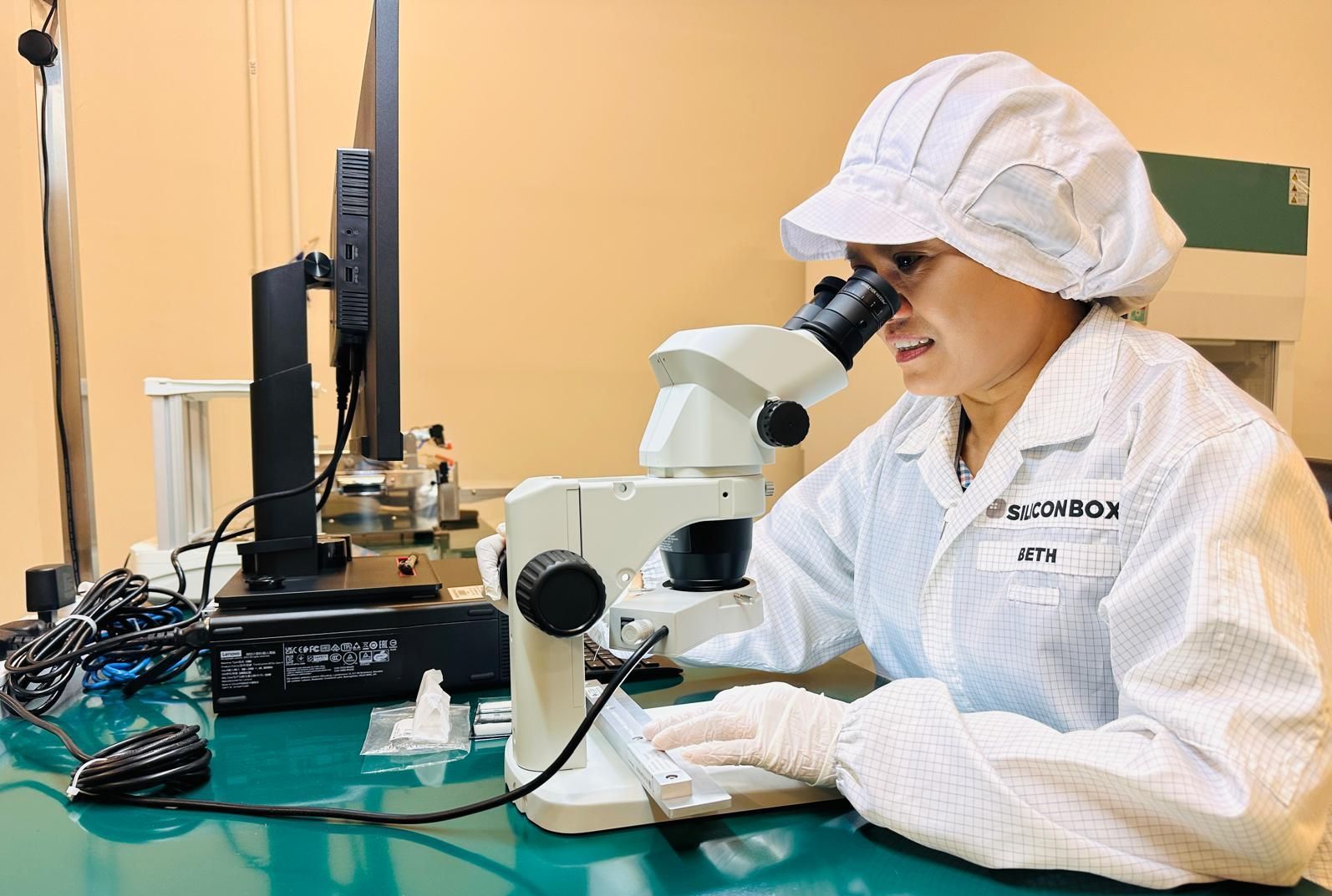
Silicon Box is an advanced semiconductor packaging company, specializing in cutting edge integration technology and manufacturing processes. We offer solutions that enable chiplet architecture, as well as high performance alternatives to traditional packaging schemes. Leveraging our proprietary technology, 30 years of multi-sectoral expertise, and relationships with best-in-class partners, we strive to solve the unique challenges of chiplet adoption in order to build the emergent technologies shaping the world around us today.
Silicon Box was founded in 2021 by Dr. Byung Joon (BJ) Han, Dr. Sehat Sutardja and Weili Dai. Dr. Han was previously the Chairman, CEO and CTO of the world’s 3rd largest outsourced assembly and test provider, STATS ChipPAC (SSE: 600584) for two decades, taking the company to $4B in revenue during his tenure. Dr. Han is the inventor of many of the most advanced packaging solutions in today’s market, and his team at Silicon Box holds standing records for yield in advanced packaging technology at wafer-level production. Dr. Sutardja introduced the concept of chiplets at the International Solid State Circuits Conference (ISSCC) in 2015. He and Weili Dai founded Marvell Technology Group (NASDAQ: MRVL) in 1995, and ran the company for twenty years from a start-up to an over $50B market value company.
To learn more about Silicon Box go to:
silicon-box.com/newsroom and
silicon-box.com