
Our Singapore factory's ISO 9001:2015 certification in 2024 is a testament to our unwavering commitment to quality and customer satisfaction. This international recognition demonstrates our ability to consistently meet customer standards and regulatory requirements. We are also proud to be ISO14001:2015 and ISO45001:2018 certified, underscoring our commitment to sustainability management, and health & workplace safety.
How are chiplets leading the semiconductor design revolution?
Semiconductor integration creates a more complex system that offers enhanced performance, improved power efficiency, and reduced form factor. It involves the integration of diverse technologies, such as digital logic circuits, analog circuits, sensors, memory elements, power management units, and more.
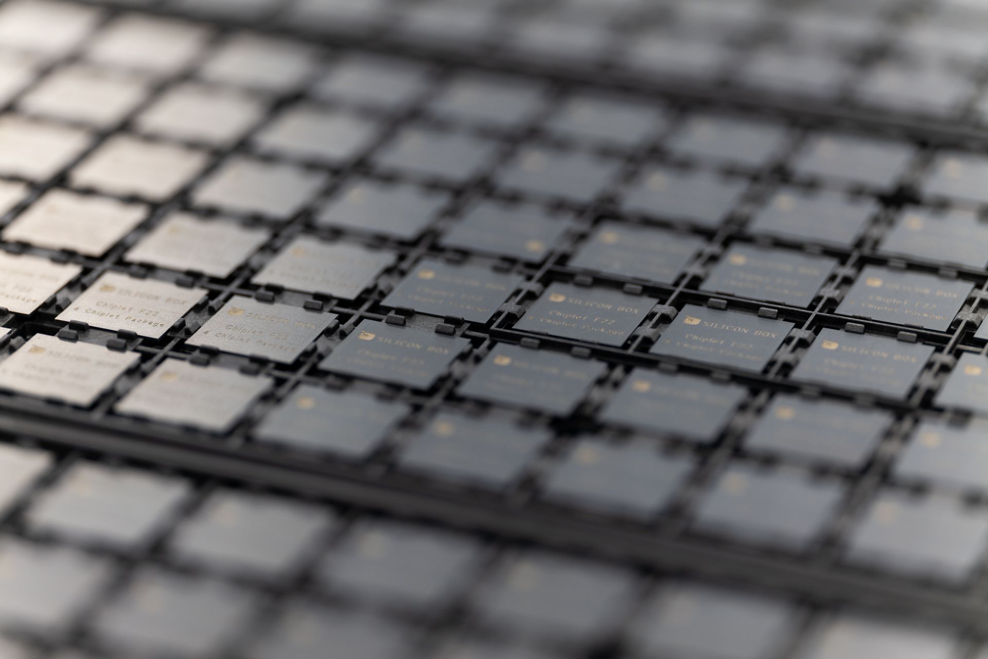
Chiplets play a crucial role in semiconductor integration.
A chiplet is a discrete, self-contained semiconductor component that performs a specific function or hosts a specific technology. Chiplets can be designed, manufactured, and tested independently of each other, and then combined or interconnected to form a larger and more complex integrated circuit.
Silicon Box’s proprietary fabrication method uses sub 5 micron technology , delivering one of the shortest interconnections in the industry and solving the unique challenges of chiplet adoption.
- Interconnect density: As chiplets become smaller and more densely packed, there is a need to accommodate a higher number of connections within a limited space.
- Power efficiency: With sub 5 micron technology, it is possible to optimise power usage by reducing resistive losses and minimising parasitic capacitance between chiplets.
- Signal integrity: The use of sub 5 micron technology helps mitigate signal degradation issues by minimising crosstalk, reducing noise, and improving overall signal quality, leading to enhanced performance of chiplet-integrated devices.
- Thermal management: Heat dissipation is a significant challenge in densely integrated chiplets. Our sub 5 micron technology enables the design and fabrication of more efficient thermal management structures, such as microchannels and heat sinks.
- Design Flexibility: Sub 5 micron technology allows for the integration of diverse chiplets with varying sizes, functionalities, and interfaces, enabling tailored solutions for specific use cases.
Our advanced chiplet integration technology sets an unmatched standard for design flexibility and electrical performance at low cost and power consumption. This agility in semiconductor design cycles enables the industry to effectively and efficiently scale chiplet-based solutions across the semiconductor value chain.
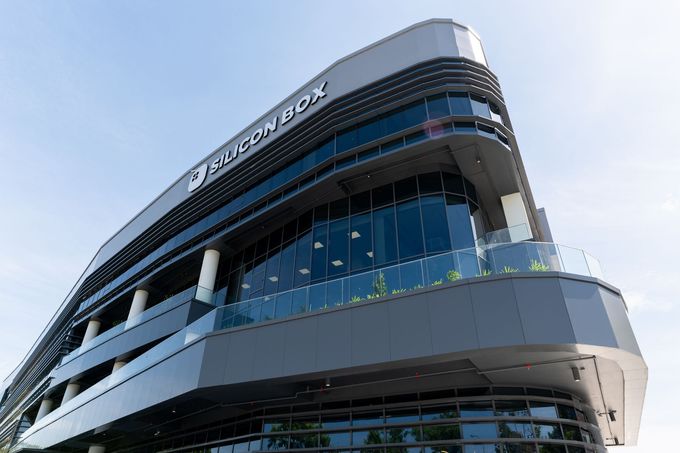
Our Factory
Our newly opened foundry is the most advanced interconnection factory in the world. Located in Tampines, Singapore, spanning 73, 000 square metres in total size, with 30, 000 square metres of production space, the factory runs on self-contained CUB power, water, gas, and thermal resource management facilities.
In keeping with industry best practices and Singapore’s requirements around sustainability, the $2 billion advanced semiconductor manufacturing foundry is built with resource efficiency in mind.